Random features in nanoscale photonic cavities can help miniaturize devices that control optical data
Published online 28 July 2016
Photonic waveguides fabricated using a speedy nanoscale patterning technique known as photolithography have more errors than a perfectly designed structure would, but can also tap into chaotic light-trapping capabilities.
Reproduced, with permission, from Ref. 1 © 2016 Optical Society of America
Researchers usually try to avoid structural flaws when constructing photonic devices that manipulate, amplify, and switch signals from light beams. A team from Japan, however, now reports a high-speed photonic system that uses random fabrication errors to localize light for more compact optical devices1.
Computing and shuttling data with light instead of electrons can hugely boost the speed and energy efficiency of signal processing. Such applications require strong interactions between photons and silicon crystals to produce nonlinear effects. One way to focus light waves at atomic targets is with photonic waveguides: ordered arrays of circular dimples, hundreds of nanometers wide, carved into a silicon surface one by one through a technique called electron-beam lithography.
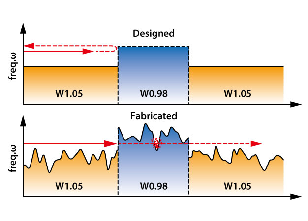
For the past decade, Takasumi Tanabe from Keio University and colleagues have been developing waveguides with strong light-confinement capabilities. One of the team's most efficient designs sandwiches one waveguide, compressed to 98% of its normal spacing (W0.98), between two others at 105% spacing (W1.05). This setup causes photons at a specific 'cutoff frequency' to propagate very slowly through the waveguide, interacting with many silicon atoms along the way.
To better integrate their W1.05-W0.98-W1.05 device with electronic silicon circuits, the researchers investigated whether it could be produced using photolithography ― a speedy way of forming nanoscale patterns using masks and etching solutions. These experiments produced dimples with larger fabrication errors than hoped for, but also modified the character of the propagating light so it became dominated by random scattering effects (see image).
Tanabe explains that when randomness increases in a photonic structure, scattering can cause light to localize and form 'nanocavities' that offer high confinement. This localization could be used to make photonic devices much smaller, but only if the randomness can be controlled by some method.
To accomplish this, the researchers varied the width of the W0.98 portion of their waveguide nanocavities until localized resonances due to randomness appeared close to the cutoff frequency. The design confined randomized light to the central region of the waveguide, and yielded sufficient optical power for practical applications. As proof, the team integrated the random photonic system into a semiconductor diode circuit to produce a device that modulates electro-optic signals at high-speed gigahertz rates.
"Our device has a much smaller footprint than conventional modulators and is compatible with photolithographic fabrication," says Tanabe. "By studying this random behavior in more detail, we might be able to develop different devices such as all-optical switches or logic gates."
Reference
- Ooka, Y., Daud, N. A. B., Tetsumoto, T. & Tanabe, T. Compact resonant electro-optic modulator using randomness of a photonic crystal waveguide. Optics Express 24, 11199 (2016). | article